(excuse crappy quality of photo)
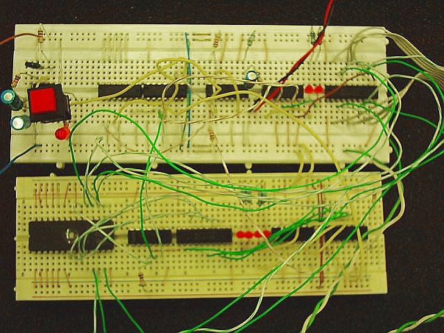
During my TAFE studies of 2004, I designed and built an
"Instruction Fetcher". Anyone that has studied computer sciences would
have heard of this term. It is a part of a computer's Central Processing
Unit (CPU) that is in charge of loading an instruction. Here is an
overview of how it works. Please refer to my hand drawn schematics:
(excuse crappy quality of photo)
- At the heart of this circuit is the "Machine Cycle Sequencer". It is the
device that sequences various logic groups to activate, perform a job
and then go dormant. It consists of a 74HC74 dual D type flip-flop and
an 74HC164 shift register.
- The 74HC74 flip flop has been configured to "init" with /Q high. When it is clocked, /Q will go low.
- The 74HC164 when inited will have all it's Q outputs low, and have Dsb high. This is the start condition. When the first clock pulse triggers this device, the state of Dsb will load into Q0. Q0 will go high.
- When Q0 goes high, it then clocks the 74HC74 flip-flop. This sets /Q low. The /Q output (of FF) will not go high again.
- As clock pulses continue into 164, The high state will move along the Q outputs. This will control our machine states.
- The 74HC161 is a 4 bit counter that stores our IP pointer (IP register).
- The fetcher will read an 8 bit instruction stored on the 27C256 EPROM (at the address stored in the IP register), and save it into the 74HC373 latch which is our instruction register (I register). The instruction register would then be used by further logic (of later machine cycles) to sense/decode the instruction and activate the code responsible to execute it.
- When MC = 0 (Machine cycle number), The Q0 output will switch the 74HC244 tristate buffer to enable it's "1Y" outputs. This makes the IP address value available on the address inputs of the 27C256. It also asserts the /CE and /OE pins of the 27C256 EPROM which enables it. The EPROM's internal circuitry will then be in the process of sensing, propagating it's internal signals, undergoing it's own execution contexts to finally make the memory value available at the "O" outputs.
- When MC = 2 (Q1 = high), the 27C256 EPROM will have had enough time to resolve the memory address and make it available at it's outputs. This data will then be available at the "D" inputs of the 74HC373 latch (I register). The high driving Q1 latches the data at the "D" inputs into it's internal flip-flops. The instruction is hence stored in the I register.
- When MC = 2 (Q1 - high), it also drivers CP pin of the IP pointer counter. This increments the IP pointer.
- The Q1 = high state also sets the MSC_RESET rail high, which causes the Machine Code Sequencer to reset.
- The whole cycle is restarted and the next instruction is loaded from memory.
- The 4 address lines going from the 74HC244 to the 27C256 is the "Address bus".
- The 1 line going from the tristate buffer's NOR gate to the /CE and /OE pins of the 27C256 is the "Control bus".
- The 8 data lines going from the 27C256 to the I register is the "Data Bus".
* * * *
The build took me a day to design on paper and a day to build. The circuit worked straight off with no modification. I haven't designed a fetcher before ; This is my own design. I assume that other implementers have followed a similar design as it seems an obvious one. However, my ideas are loosely based on a digital sequencer I had to build in year 12 electronics matriculation assessment (1989).
Building this has given me an appreciation of what computing was like prior to 1970. With a bit of time and patience, it wouldn't be that hard to completely build a full working CPU using discrete logical components like the 74xx series I have used in this assessment.